Etching single and double sided PCBs
Posted on December 16th, 2016
This is going to be a quick post about how I etch PCBs and more importantly my recent experience with double sided PCBs. I won’t go into too much detail but I am going to try and provide some useful tips I found along the way.
Designing your PCB
There are a lot of programs out there for designing PCBs such as Eagle and DipTrace which are high quality professional solutions for design PCBs. I have tried a few of these when getting PCBs manufactured but the learning curve is steep. However, there is a great (and popular) piece of software called the DIY Layout Creator created by a member of the DIY stomp box community called banika. I would highly recommend this for a first time user or hobbyist who just wants to design and etch a board. It has a great intuitive UI and can also be used for veroboard layouts and schematics. DIY Layout Creator can be found here http://diy-fever.com/software/diylc/
Transferring your design onto copper
There are a couple of options to get your design onto the copper board such as screen printing and photo resist methods. However, I am going to talk about the toner transfer method which is very popular and (in my experience) produces good results. The toner transfer methods works by printing your design onto a medium using a laser printer and then using heat to transfer the toner onto the copper.
Picking your paper
The key to this is picking a suitable paper so that the toner comes away easily. There are a few commercial and DIY options, the three I have used are:
- Blue press and peel – I have had mixed success with this, it is fairly expensive and I found you had to get the temperature correct for it to transfer
- Yellow PCB paper – I found this very cheaply on eBay. The paper is a yellow glossy almost waxed paper. This is my preferred paper, the toner comes away easily but that does mean it can rub off.
- Glossy Photo Paper\Magazine paper – This is possibly the cheapest and easily available option. However I have had mixed success with this option. I found that the success varied dramatically with different paper so be prepared to try lots of different types. I found thin glossy magazine paper worked best.
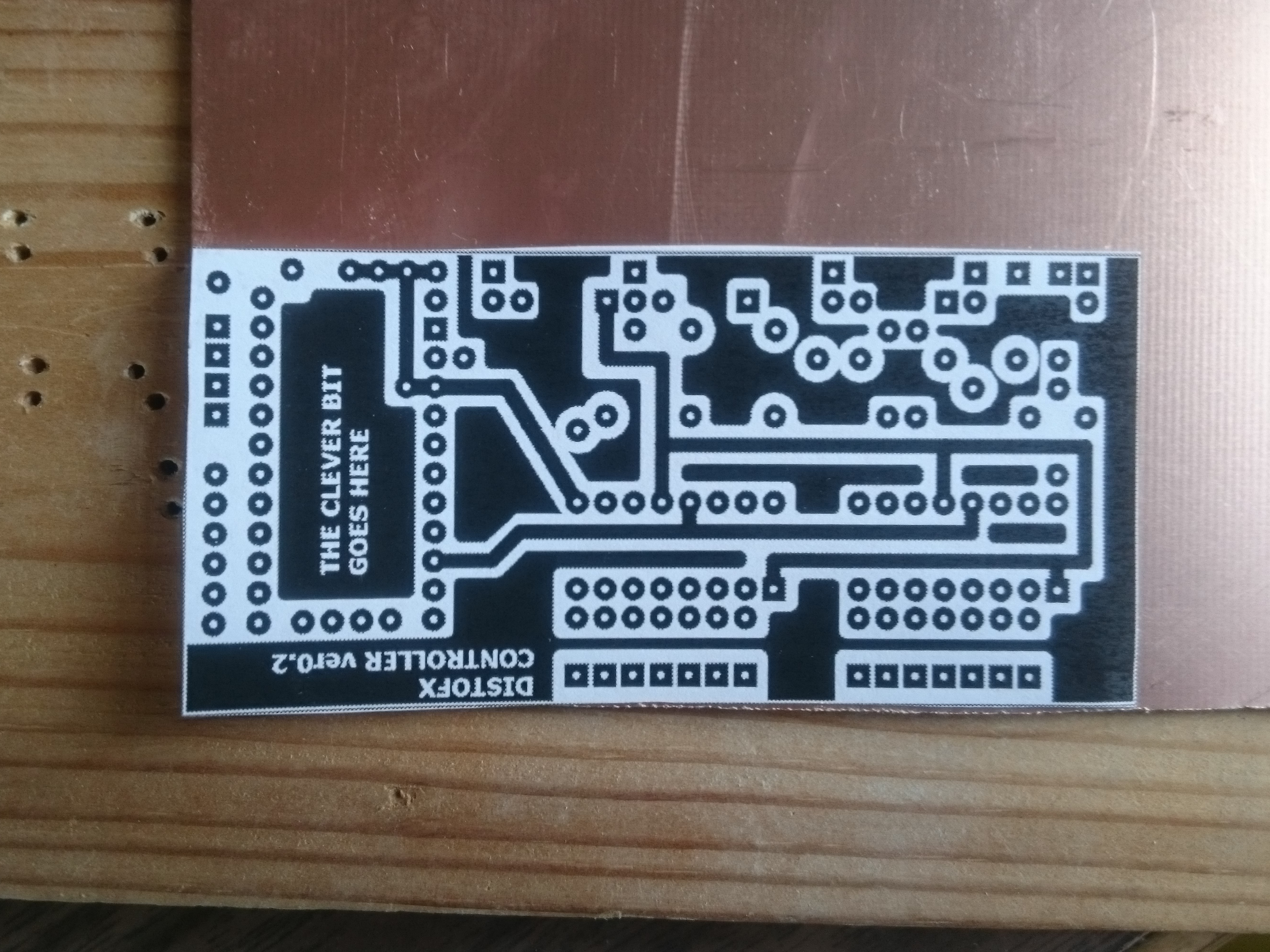
Remember that the design needs to be printed in reverse
Preparing the board
Before you transfer the toner you need to cut the copper board. Either mark the board outline using a pen\pencil or cut out a copy of the design onto normal paper or card and use this as a template. You could use a glue stick to temporarily hold the paper onto the board. Before transferring the toner, it is important to remove any oils or marks from the board. Clean the board using fine wire wool and a some lighter fluid.
Marking up the design ready to cut the copper board
Transferring the toner
To transfer the toner you need to apply heat and pressure. I have seen some people use a laminator but I find an iron works well. Once you have the the design printed onto the transfer paper cutout the design and align it carefully on the board, you can use masking tape to keep it in place but I find just applying a little bit of heat with iron to get it to start sticking also works.
I find placing the board on a solid surface (this is important) such as some wood and the covering with baking paper and then applying the iron with some pressure helps the process. Keep moving the iron across the board and make sure you apply heat to the entire board. I like to use the tip of the iron in a rubbing motion to make sure I have covered the entire board and then the flat of the iron to apply an even heat. The time need may vary but I tend to keep the iron on for a few minutes.
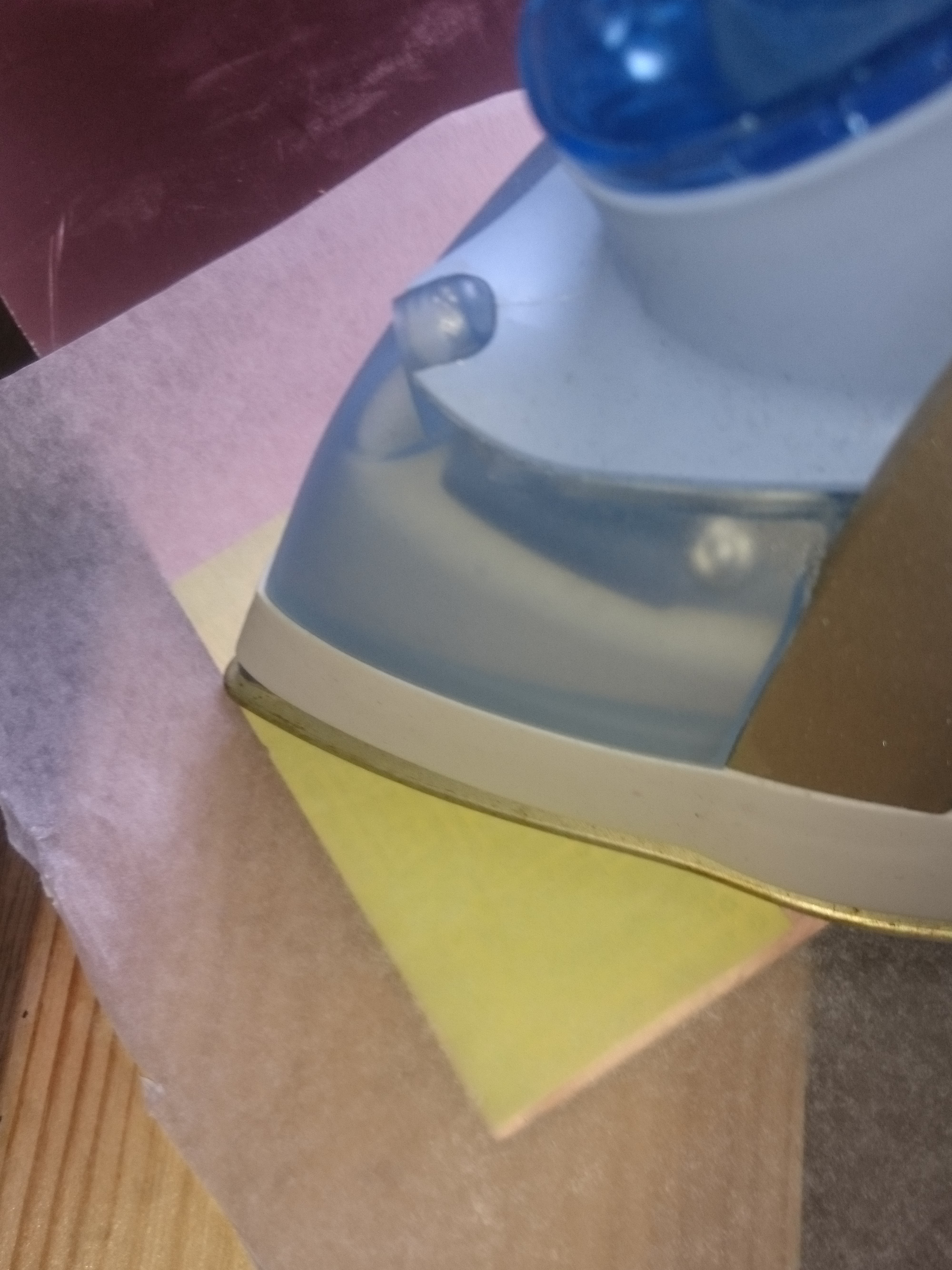
Transferring the toner onto the PCB

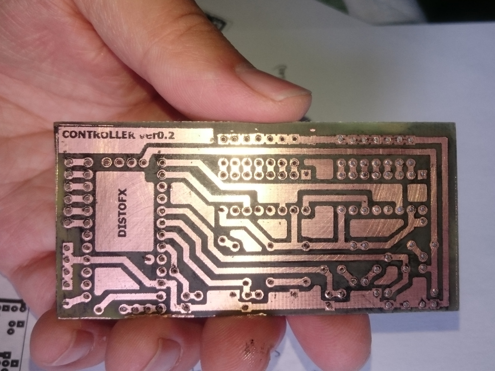
The PCB board after the toner has been transferred
Once you have applied the heat cool the board in water, be careful as it will be hot. Once the board has cooled you should be able to peel the paper off leaving the toner on the copper, carefully rubbing to remove any left-over paper. You may need to touch up some areas using a permanent marker such as a CD pen or Sharpie.
Etching
Once you have transferred your design onto the board it is time to start etching. For the etching process I use ferric chloride but I have heard that caustic soda (Sodium hydroxide). Ferric chloride can be nasty stuff and needs to be disposed of carefully. Take precautions an wear eye protection, gloves and old clothing. Pour the ferric chloride into a plastic container, I tend to use a small tub just larger than the PCB I am etching. I then fill a larger container with warm water from a kettle and sit the tub containing the ferric chloride into the warm water. This works like a heat bath and will speed up the process. I carefully place the PCB in the ferric chloride and agitate the tub to ensure that the PCB is submerged. Remember that ferric chloride reacts with metal so you must use non-metal containers and stirring implements. Continue to agitate the ferric chloride, checking the progress of the PCB periodically. After a few minutes you should see the PCB changes colour and eventually you will start to see the copper completely disappear. The areas cover by the toner should not be removed by the ferric chloride, the toner can be removed later, leaving the copper behind. Once the copper has all been etched away, remove the PCB from the ferric chloride and rinse in water to stop the reaction. Dry off the board and you are ready to drill the holes. Once I have finished etching I put the ferric chloride back in the bottle and use again next time.
Drilling the holes
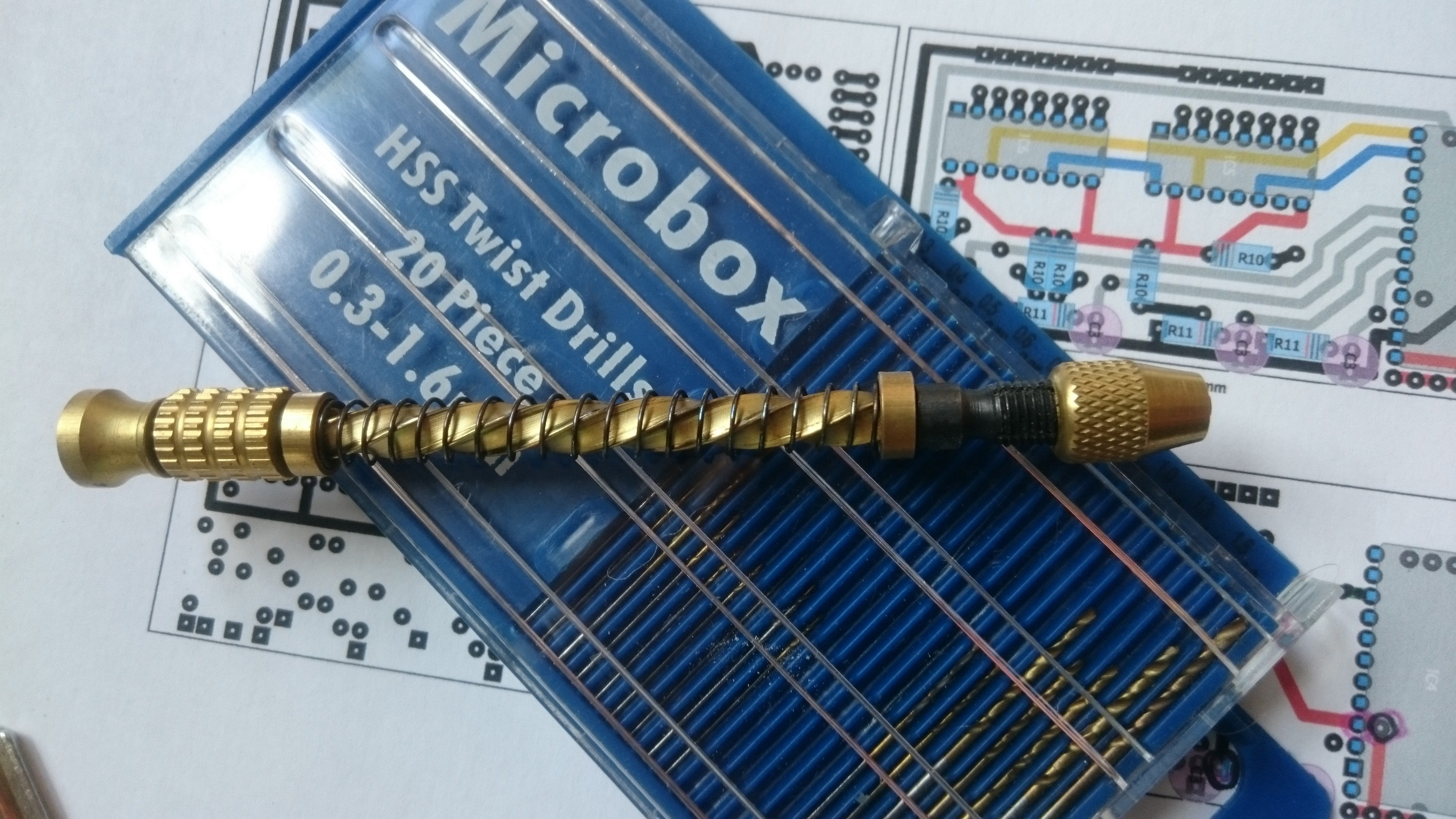
I haven’t yet decided on the right size holes to drill but I tend to use a drill bit around 1mm to 2mm. I would however, suggest stocking up on drill bits. Because the drill bits are so thin I found it was far to easy to break a bit. If you are only making a small board with a small number of holes, a hand Archimedes drill will work nicely. However, it’s easy to break a bit. If you are drilling a lot of holes I would recommend using a bench-top drill stand. Once you have drilled the holes, remove the toner using nail polish remover. Before you solder you can use steel wool and lighter fluid to make sure the PCB is clear.
Hand Archimedes drill
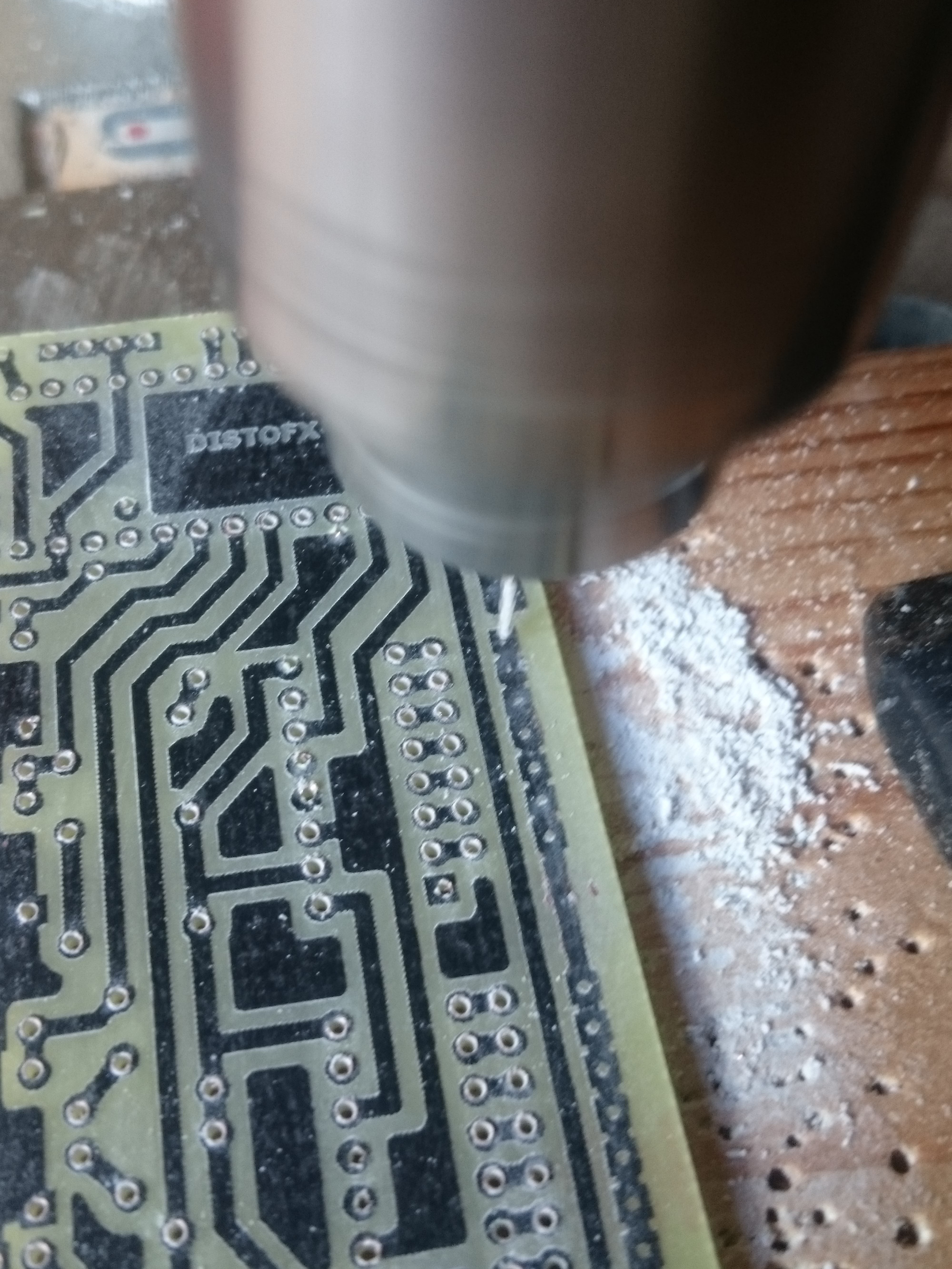
Drilling holes in a PCB using a drill press
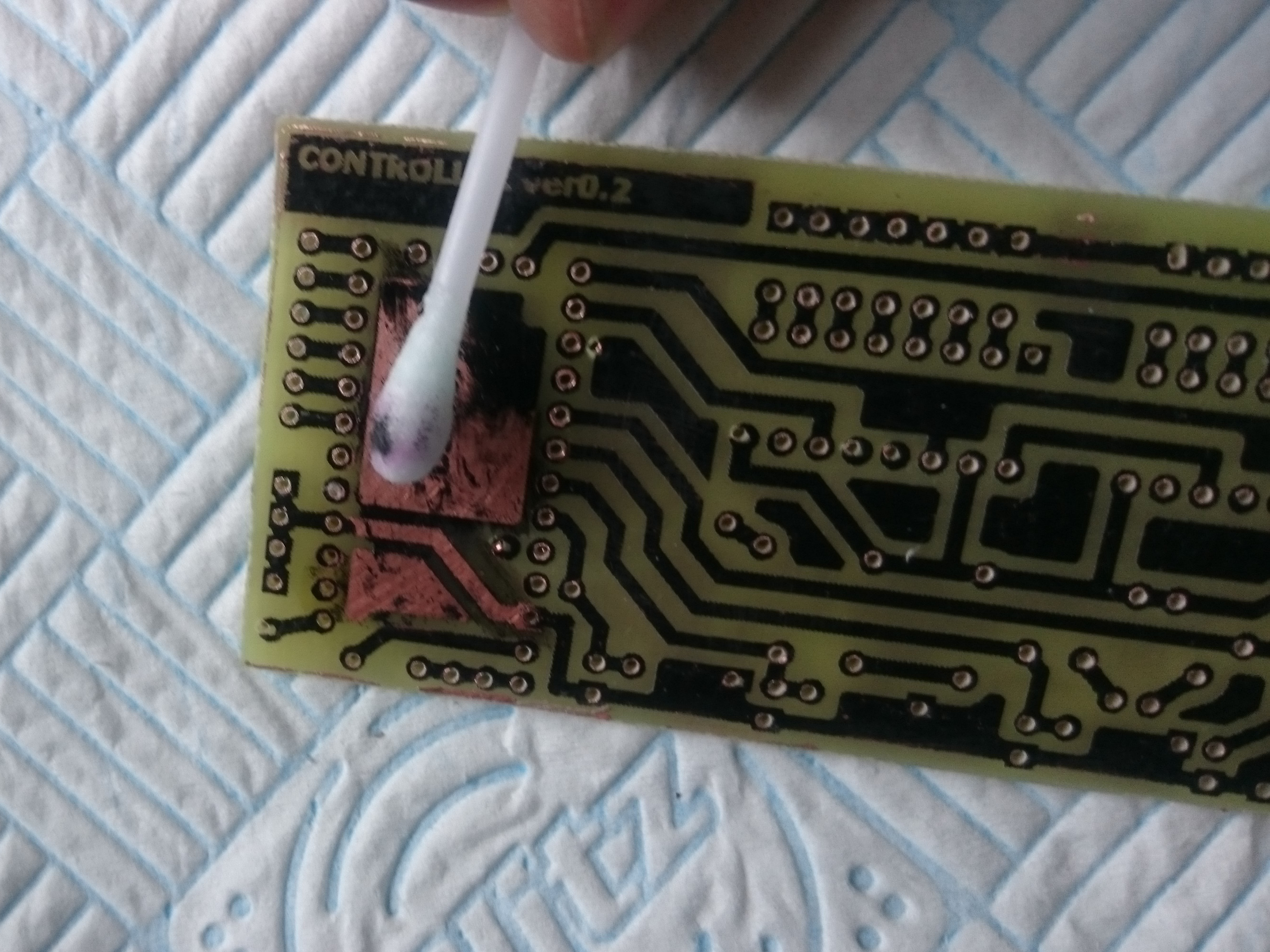
Removing the toner after etching and drilling
The finished PCB
Double sided PCBs
The process is the same for double sided PCBs, a double sided PCB may make it easier to create compact PCBs for more complex designs. The only difference in the process is that you will need to transfer toner to both sides of the PCB and this will require careful alignment. I have a few tips to ease the process.
- Allow for misalignment, use large pads and leave plenty of gaps between pads and traces. This will hopefully avoid accidentally connecting pads or traces if the layers are not perfectly aligned
- Whilst you can put pads on both sides I would avoid this. Only put pads when they are needed and only use pads on both sides if you are creating a via (a connection from one side to the other)
- Use some kind of alignment marker. One option would be to transfer the toner to one side, drill an alignment hole and then use this whole to align the toner on the other side
I hope this post provides some useful advice for etching your own PCBs. It’s certainly a rewarding process when you finally complete your own PCB.


